Develop optimized IC Design with us
Guiding you through the IC Design process, to achieve efficient and optimized design
Our Full-Scale VLSI Design
✔ RTL Design & Microarchitecture – High-performance, power-optimized RTL development for ASICs and FPGAs.
✔ Custom Layout & Physical Design – Precision-driven floorplanning, placement, and routing for analog, digital, and mixed-signal ICs.
✔ DFT Design For Testability - Structured DFT methodologies to improve test coverage, fault detection, and production yield.
✔ Circuit Design & Simulation – Robust schematic design, SPICE simulation, and transistor-level optimization.
✔ Design Verification (DV) – Comprehensive UVM/OVM-based verification, formal verification, and emulation to ensure first-time-right silicon.
✔ Tapeout & Yield Engineering – Proven methodologies for DRC/LVS-clean tapeout and manufacturability.

RTL
Our new team of RTL engineers is growing their experience with theoretical and in-house projects.
- Our RTL engineers craft power-aware, timing-optimized logic that balances performance (PPA) with verification complexity. We specialize in:
- Low-latency data paths & power gating
- Formal property checks for early bug detection
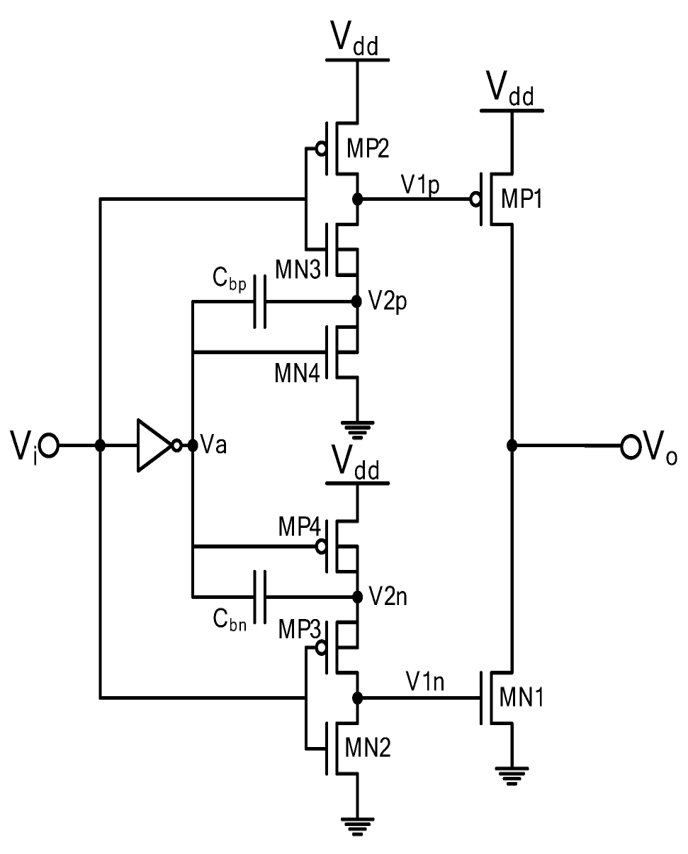
Circuit
We have an analog circuit design team with over 14 years of experience and multiple successful tapeouts across diverse technologies. Our expertise spans high-performance analog and mixed-signal solutions tailored to meet complex design challenges
Circuit Design (Blocks + Full Chip):
- Amplifier - Single Stage Amplifier, OpAmp
- Biasing Block - Beta Multiplier, BGR, LDO, Droop Injector
- Low Speed Transceiver – RS485, CAN
- Clocking Circuit – PLL, Programmable Delay Controlled Oscillator
- Data Converter – Flash ADC
Simulation:
- AC, DC, Transient, Phase Noise, Aging, EMIR
- Post Layout simulation using “config” view
- AMS simulation containing Verilog-A block
Verification:
- IP test
- PPA optimization
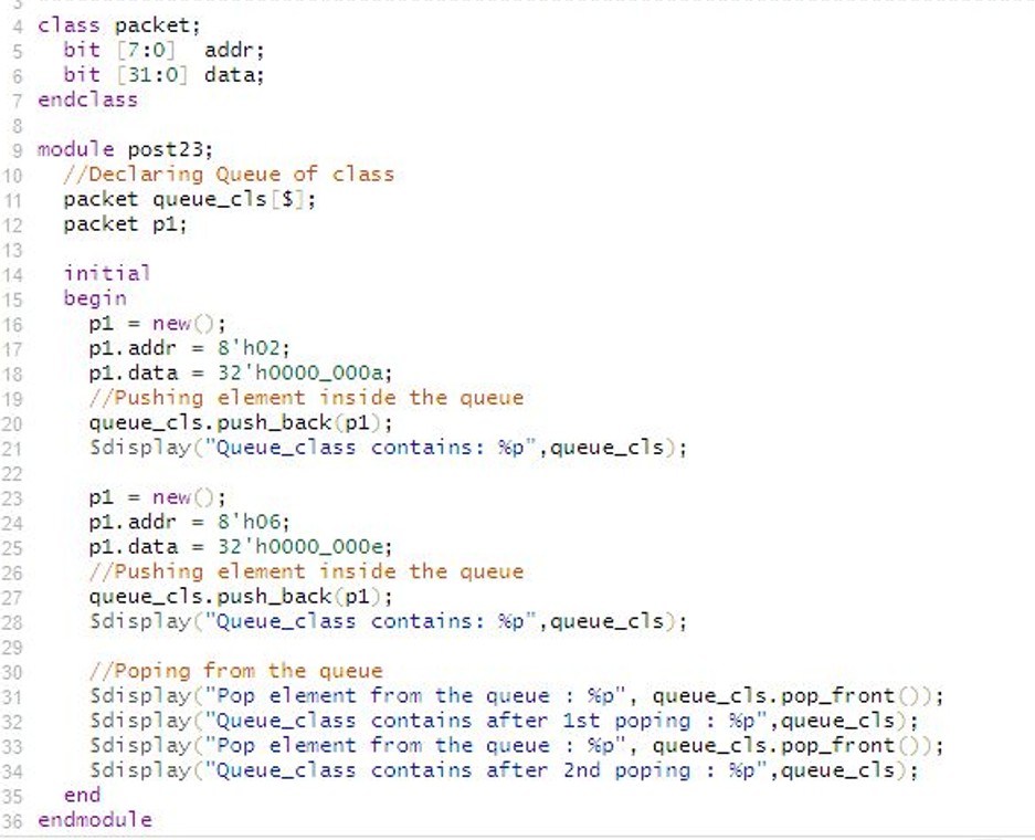
DV
Our DV team builds bulletproof testbenches using UVM, AI-driven coverage closure, and formal verification. We specialize in:
- Verilog, System Verilog, and UVM
- Reusable verification IP
- UVC development for different protocols like AXI, APB, AHB.
- Functional Verification of SoC (ARM processor, Google Server chip)
- Functional Verification of IP-level
- Functional Verification of end-point devices (UART, etc)
- Functional Verification of Controller Bus Protocol
- GLS Verification of GPU sub-system, CPU subsystems (DSP)
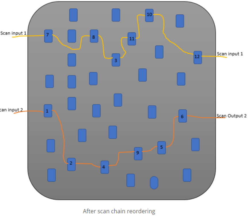
DFT
Our DFT engineers implement high-coverage, low-overhead test structures:
- DFT Planning and architecture support based on customer requirements
- Boundary scan insertion on top-level RTL
- Boundary scan pattern simulation on RTL or gate level
- Logic Equivalence check on post DFT RTL/Netlist
- MBIST Insertion on core level and top level
- JTAG UTDR Control point insertion for better DFT control on the design
- ATPG and coverage analysis to gain maximum achievable coverage of the design
- Pattern failure debugging
- Deliver production pattern for JTAG, BSCAN, MBIST, and Scan [Including multiple fault models]
- Post-Silicon support [ATE pattern failure analysis]
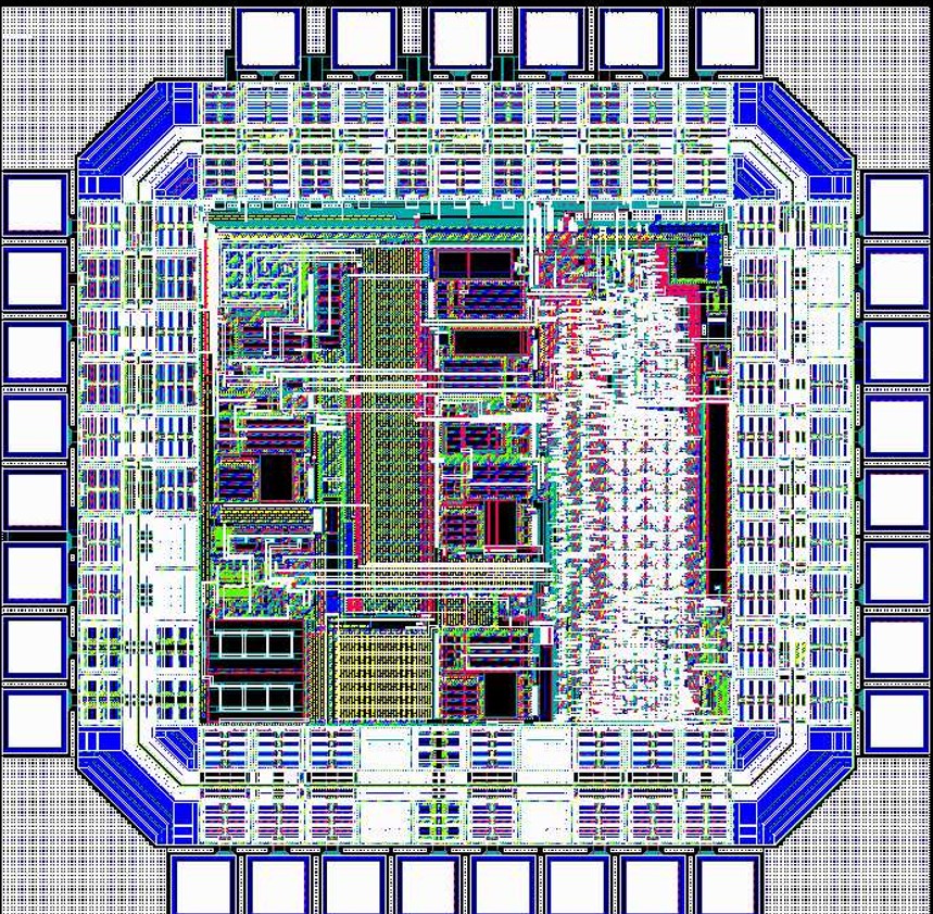
Analog Layout
Our layout team optimizes for density, signal integrity, and manufacturability:
- Technology Node Experience:
3nm, 4nm, 5nm, 7nm, 12nm, 14nm, 16nm, 90nm, 150nm, 165nm, 180nm
- Foundries:
- GlobalFoundries: 12nm, 22nm, 28nm, 40nm, 55nm, 180nm
- Samsung: 4nm, 7nm, 8nm
- Intel: 16nm
- Foundries:
- Deep N Well, Finfet design technologies
- Analog IP Layout – Power Modules, Voltage Monitor, Test Chip, OCD, and more
- Block level design – Oscillators, Transmitters, Buck-Boost converters, and more
- LVS, DRC, ERC, PERC, HIPRE, Extraction run, EM/IR
- Knowledge of analog layout techniques: Matching, Current mirror, latch up, Crosstalk, Shielding, Chip top level, Power planning, Bump connection, ESD connection, Antenna, EM/IR, Density issues, Guard ring, etc.
- EDA Tools: Custom Compiler, Virtuoso Layout XL/L, Tanner L-edit, Calibre, PVS, ICV
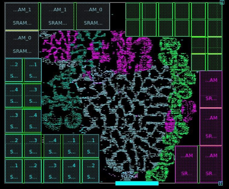
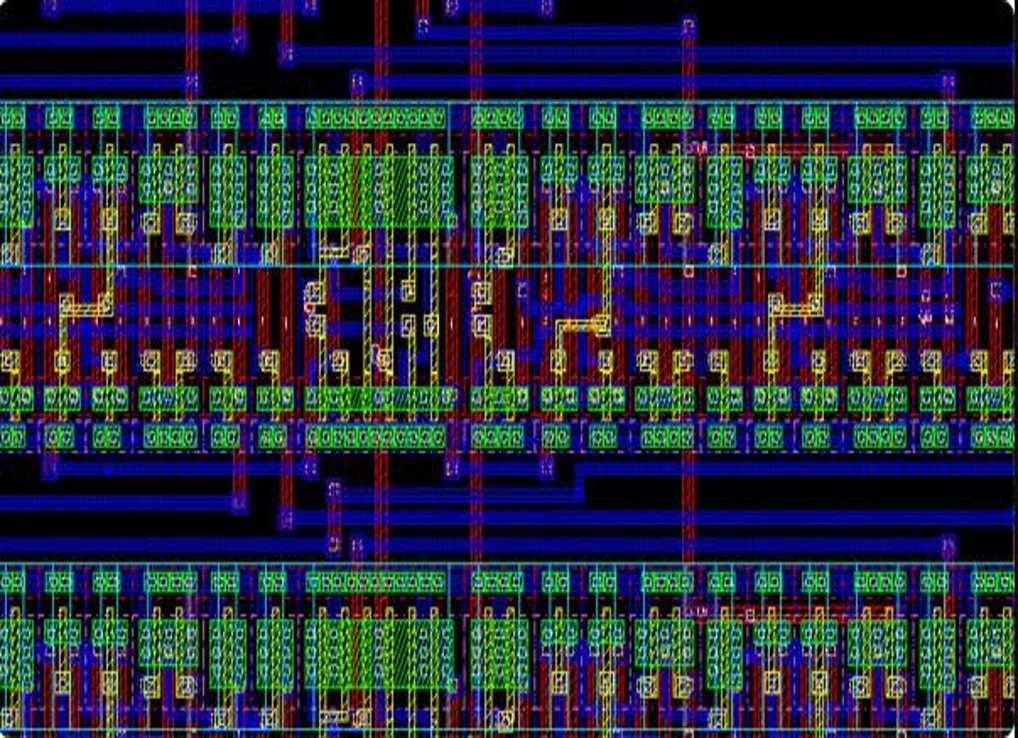
PnR
Our PD engineers conquer nanometer-scale challenges:
- Multi-corner multi-mode (MCMM) timing closure, Low-skew, low-power clock trees
- Flow Development : Synthesis (Genus, Design Compiler, Fusion Compiler), PNR (ICC2, Fusion Compiler), Design Planning (ICC2/FC), MSCTS (ICC2)
- Full Chip: Design Planing for Top-down approach to Provide block level Floorplan/IO/PG/Bumps, STA for bottom-up approach to provide block level IO/hold timing ECO and full chip signoff timing check. Global clock and Global trunk routing.
- Synthesis for hierarchical and Subchip Level Synthesis, SDC/Timing issue Debug and feedback to Frontend
- Hierarchical and Subchip Level Complete PNR from Netlist to GDS2.
- Module hierarchy and RP group based floorplan for CXL (fab), DDR Cntrl, Cortex CPU, multiple Serdeses based design
- Manual and reference clock routing/skew balance/latency adjustment/and all physical implementations for different IPS and Protocols like PCIE/DISP/DDR/NOC/CXL etc.
- Signoff-grade STA, DRC, LVS and power analysis
- Team lead for 5+ successful tapeout by Managing Schedules/issue tracking/feedback to frontend.
- Nodes 3nm, 4nm, 5nm, 7nm, 12nm, 14nm 22nm, 28nm, 40nm, 90nm